Postdoctoral Researcher
Palo Alto Research Center,
EMDL/SSL

Highly accomplished, patented Research Engineer leverages a PHD in Electrical Engineering alongside 10+ years of significant achievements in the field of Engineering, Nanotechnology and Physics, specifically instrument and sensor development, optimization, circuit design and algorithm development. Strong demonstrated interdisciplinary background in Electrical, Mechanical and Software Engineering, author of numerous publications and articles. Highly analytical, detail-oriented and committed to continuous improvement; a creative problem solver who thrives in highly collaborative, innovative research arenas.
Palo Alto Research Center,
EMDL/SSL
Ilmenau University of Technology,
Department of Electrical Engineering
Massachusetts Institute of Technology,
Department of Mechanical Engineering
Ilmenau University of Technology,
Department of Electrical Engineering
Lawrence Berkeley National Laboratory,
Advanced Fusion Research Division
Ilmenau University of Technology,
Department of Electrical Engineering
BOSCH GmbH,
Digital Circuit Design
Ph.D. in Electrical Engineering
Ilmenau University of Technology, Germany
Master of Science in Electrical Engineering
Ilmenau University of Technology, Germany
Bachelor of Science in Electrical Engineering
Trier University of Applied Sciences
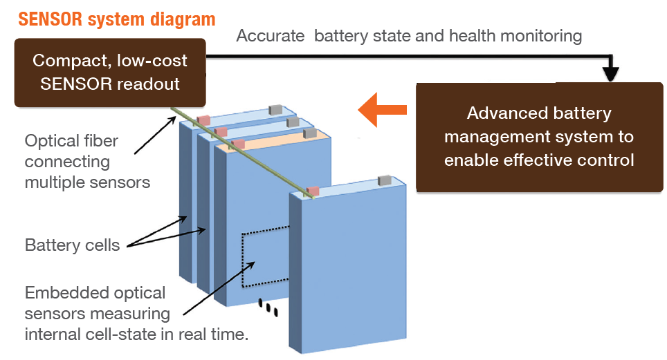
PARC has combined its novel fiber-optic sensor technology with its deep expertise in intelligent algorithms to develop a system that enables real-time measurement of a battery’s internal conditions. Fiber-optic sensors offer high performance yet are inexpensive and well-suited to the harsh environment within a battery. However their use has been limited because the read-out units are costly.
PARC’s compact wavelength shift detector is significantly smaller and less expensive than today’s read-out unit, while retaining excellent sensitivity (< 50fm). With this key enabler, fiber-optic sensors can now be costeffectively embedded into each battery cell to measure internal parameters directly. The result is unprecedented accuracy of SoC and SoH measurements to more fully utilize a battery’s potential.
Relevant publication: High-resolution, high-frequency wavelength shift detection of optical signals with low-cost, compact readouts.
High speed imaging and mapping of nanomechanical properties in atomic force microscopy (AFM) allows the observation and characterization of dynamic sample processes. Recent developments involve several cantilever frequencies in a multifrequency approach. One method actuates the first eigenmode for topography imaging and records the excited higher harmonics to map nanomechanical properties of the sample. To enhance the higher frequencies' response two or more eigenmodes are actuated simultaneously, where the higher eigenmode(s) are used to quantify the nanomechanics.
In this project, each imaging methodology is combined with a novel control approach. It modifies the Q factor and resonance frequency of each eigenmode independently to enhance the force sensitivity and imaging bandwidth. It allows us to satisfy the different requirements for the first and higher eigenmode. The presented compensator is compatible with existing AFMs and can be simply attached with minimal modifications. Different samples are used to demonstrate the improvement in nanomechanical contrast mapping and imaging speed of tapping mode AFM in air. The experiments indicate most enhanced nanomechanical contrast with low Q factors of the first and high Q factors of the higher eigenmode. In this scenario, the cantilever topography imaging rate can also be easily improved by a factor of 10.
Relevant publication: Multi-eigenmode control for high material contrast in bimodal and higher harmonic atomic force microscopy.
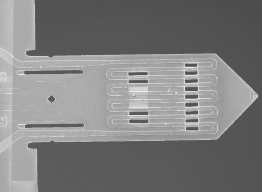
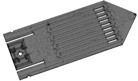
Atomic Force Microscope probes are mechanical beams that can be used to simultaneously map topography and material properties. Upon contact of the tip with the sample surface at each cycle in the intermittent mode, higher harmonics are excited. The harmonics in the vicinity of higher eigenmodes are enhanced and present an amplified response, ultimately carrying information about the material properties.
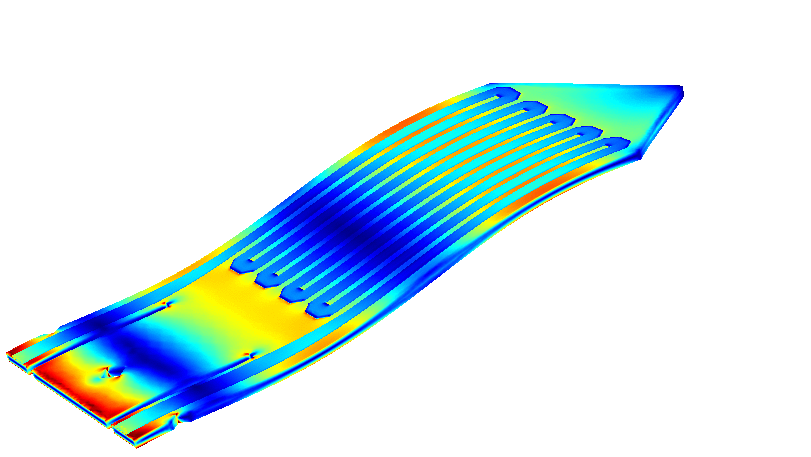
In this project, active cantilevers with integrated actuation and sensing are used as a basis to create harmonic cantilevers for the Signal-to-Noise Ratio improved measurement of time-varying forces. Focused Ion Beam milling is used to remove mass from specific areas in the cantilever such that the fundamental and higher eigenmodes are tuned towards each other. Two methods are tested, where the shape and location of mass removal is determined, first, by simulation and, second, through an in-situ approach. Higher harmonics of the harmonic cantilevers with piezo-resistive deflection sensors indicate a significant response of up to 10% in respect to the first harmonic. The improved material contrast mapping abilities of the modified cantilevers are validated by characterization and AFM images.
Relevant publication: Active microcantilevers for high material contrast in harmonic atomic force microscopy.
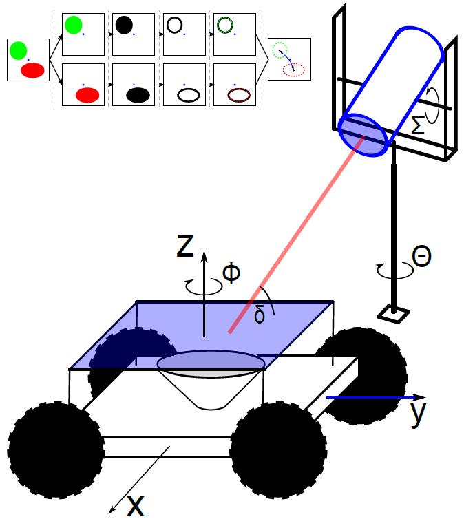
Reliable tracking and localization methods of mobile robots are necessary for the inspection process of Liquefied Petroleum Gas tanks. Lacking alternatives, humans have been sent into these tanks under hazardous conditions, resulting in substantial financial losses due to extended shutdown periods. Mobile robot platforms can be used to conduct this work, replacing the human interaction. We introduce a laser based tracking and localization technique to guide the robots within the tanks.
The tracking concept utilizes standard components and proofed detection techniques to find the parameters of laser beam shapes on the robot screen. The choice of red and green lasers turns out to be very handy, since the two lasers can be easily differentiated by splitting the captured images into their RGB color channels. Combining the information of the robot laser detection, the gimbal angles and the laser distance measurement allow local and global localization of the robot in four DOF.
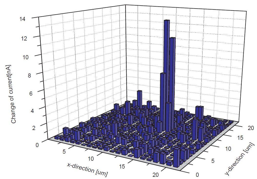
Quantum computing devices realized in silicon based solid states require precise placement of single donors within the lattice of the target. Accumulation field effect transistors are a possible target device and single ion impacts can be detected by different effects like a varying channel current due to a mobility change of charge carriers.
This project addresses the detection of recorded current changes via a Kalman filter with an automatic parameter estimation. Automatic alignment of the active area with small collimating holes drilled into the cantilever of an Atomic Force Microscope (AFM) is possible with the filter implemented in a LabVIEW program. These holes allow single ion transmission and by scanning the tip above the surface, low energy 20-50 keV ions can be implanted into cells within a predefined array.
The detection algorithm has been successfully tested on recorded single ion hits generated by pulsing the ion beam. Mapping of ion beam induced current changes has been done with the implemented LabVIEW program and the integrated AFM. A response was visible, when the holes were aligned to the channel of the transistor.
Journal/Conference Papers, Unpublished Work, Reports and Theses.
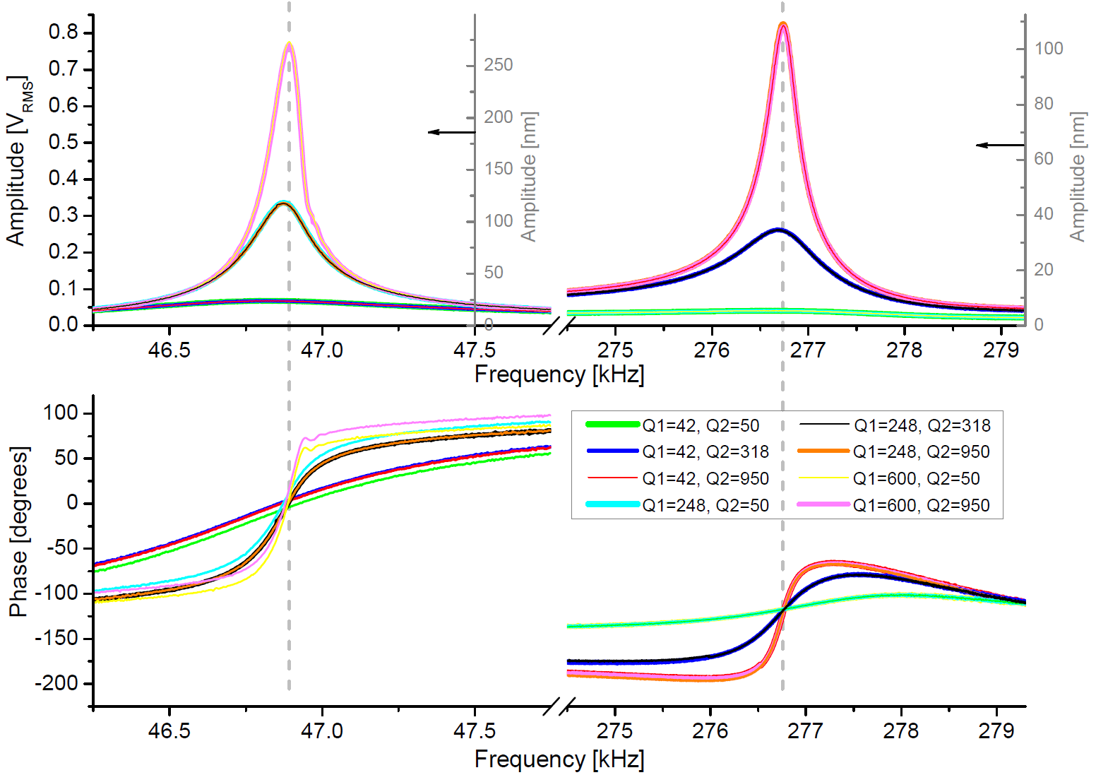
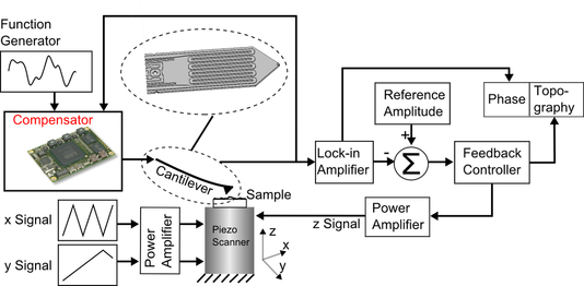
High speed imaging in Atomic Force Microscopy (AFM) tapping mode depends on the cantilever’s effective resonance frequency and Q factor. Imaging in higher cantilever eigenmodes implies increased acquisition bandwidths based on the frequency. However, in combination with the corresponding Q factor it leads to a specific time constant of each eigenmode. The detection and control of the higher eigenmodes has become easily available with the development of powerful data acquisition and processing hardware. To achieve a greater flexibility, we apply a control methodology that arbitrary modifies the cantilever dynamics. It results in the modification of both Q factors and resonance frequencies. Using higher eigenmodes in combination with lowered Q factors considerably enhances the image acquisition rate. A 20 times increase in imaging bandwidth is achieved by using the presented methodology. On the other side, the resolution can be enhanced by using increased Q factors. The modification of the resonance frequency (F control) allows imaging at resonances that are not natural to the cantilever. The design of the single eigenmode compensator is outlined and applied as a simple modification to an AFM characterization and imaging environment. The performance is evaluated on different samples in tapping mode in air.
Atomic Force Microscope probes are mechanical beams that can be used to simultaneously map topography and material properties. In particular the imaging speed and force sensitivity are major concerns that often require a trade-off approach. In this work, a novel estimator based multi-eigenmode compensator is introduced to modify the dynamics of each resonance independently. Modeling, compensator design, implementation strategy in a digital system and validation in experiments will be presented. A single-eigenmode version of the compensator is used to modify the Q factor of the first three eigenmodes separately. Using higher eigenmodes in combination with a modified Q factor leads to a 20-fold increase in image acquisition rates. The modification of the natural frequency (F control) allows imaging at resonance frequencies that are not natural to the cantilever. The emerging multifrequency Atomic Force Microscopy utilizes higher eigenmodes to improve imaging speed and force sensitivity concurrently. One method actuates the first eigenmode for topography imaging and records the excited higher harmonics to map a sample’s nanomechanical properties. To enhance the higher frequencies’ response two or more eigenmodes are actuated simultaneously, where the higher eigenmodes are used to quantify the nanomechanics. In experiments, the compensator is used to specifically modify the Q factors of the cantilever’s first two transversal eigenmodes concurrently in both imaging schemes. The experiments indicate most enhanced material contrast and imaging rate with low Q factors in the first eigenmode and high Q factors in the higher eigenmode. An extension of the compensator allows for a high speed Lock-in amplifier free amplitude demodulation, which is used for topography imaging with the first resonance. A different technique for improving material property sensitivity is presented based on structural modifications of the cantilever. Focused Ion Beam milling is used to remove mass from specific areas in the cantilever such that the first and higher eigenmodes are tuned towards each other. The shape and location of mass removal is determined either by simulation beforehand or through an in-situ approach. Higher harmonics of the harmonic active cantilevers indicate a significant response of up to 10% in respect to the first resonance/harmonic.
High speed imaging and mapping of nanomechanical properties in atomic force microscopy (AFM) allows the observation and characterization of dynamic sample processes. Recent developments involve several cantilever frequencies in a multifrequency approach. One method actuates the first eigenmode for topography imaging and records the excited higher harmonics to map nanomechanical properties of the sample. To enhance the higher frequencies' response two or more eigenmodes are actuated simultaneously, where the higher eigenmode(s) are used to quantify the nanomechanics. In this paper, we combine each imaging methodology with a novel control approach. It modifies the Q factor and resonance frequency of each eigenmode independently to enhance the force sensitivity and imaging bandwidth. It allows us to satisfy the different requirements for the first and higher eigenmode. The presented compensator is compatible with existing AFMs and can be simply attached with minimal modifications. Different samples are used to demonstrate the improvement in nanomechanical contrast mapping and imaging speed of tapping mode AFM in air. The experiments indicate most enhanced nanomechanical contrast with low Q factors of the first and high Q factors of the higher eigenmode. In this scenario, the cantilever topography imaging rate can also be easily improved by a factor of 10.
Atomic force microscope (AFM) probes are mechanical beams that can be used to simultaneously map topography and material properties. Upon contact of the tip with the sample surface at each cycle in the intermittent mode, higher harmonics are excited. The harmonics in the vicinity of higher eigenmodes are enhanced and present an amplified response, ultimately carrying information about the material properties. In this paper, active cantilevers with integrated actuation and sensing are used as a basis to create harmonic cantilevers for the signal-to-noise ratio improved measurement of time-varying forces. Focused ion beam milling is used to remove mass from specific areas in the cantilever such that the fundamental and higher eigenmodes are tuned toward each other. Two methods are tested, where the shape and location of mass removal is determined, first by simulation and second through an in situ approach. Higher harmonics of the harmonic cantilevers with piezoresistive deflection sensors indicate a significant response of up to 10% in respect to the first harmonic. The improved material contrast mapping abilities of the modified cantilevers are validated by characterization and AFM images.
Today, multifrequency Atomic Force Microscopy is a popular technique to extract properties of a sample surface other than the topography through different channels. Such channels are represented by the higher eigenmodes and harmonics of the flexural vibrations of the cantilever. In one method two or more eigenmodes are actuated simultaneously, whereas another method captures the harmonics excited from the first eigenmode tapping the surface. In this paper, we present a compensation strategy to modify the dynamics of two transverse eigenmodes independently. The modeling, compensator design, implementation and imaging performance on a polymer sample is outlined. In particular low Q factors in the first and high Q factors in the second eigenmode indicate a strong improvement in material contrast mapping. As the imaging bandwidth depends on the Q factor of the first eigenmode, the imaging rate is increased simultaneously.
Fiber-optics (FO) have great potential for distributed sensing in various harsh environment applications. Their advantages include high resolution and multiplexing capabilities, inherent immunity to electromagnetic interference, and low weight/volume. However, their widespread adoption in commercial applications has been considerably limited by the high cost, size, weight, and lack of capabilities of the readout unit used to interpret the FO signals. PARC has developed a breakthrough wavelength shift detection (WSD) technology that is capable of reading out signals from wavelength-encoded FO and other optical sensors with high sensitivity using a compact, high-speed and low-cost unit. In this paper, its calibration and noise performance is demonstrated for high-resolution (up to 1,45 fm/√Hz) acoustic emission (AE) detection of fast (up to 1 MHz) dynamic strain signals.
Improved imaging rates in Atomic Force Microscopes (AFM) are of high interest for disciplines such as life sciences and failure analysis of semiconductor wafers, where the sample topology shows high aspect ratios. Also, fast imaging is necessary to cover a large surface under investigation in reasonable times. Since AFMs are composed of mechanical components, they are associated with comparably low resonance frequencies that undermine the effort to increase the acquisition rates. In particular, high and steep structures are difficult to follow, which causes the cantilever to temporarily loose contact to or crash into the sample. Here, we report on a novel approach that does not affect the scanner dynamics, but adapts the lateral scanning speed of the scanner. The controller monitors the control error signal and, only when necessary, decreases the scan speed to allow the z-piezo more time to react to changes in the sample's topography. In this case, the overall imaging rate can be significantly increased, because a general scan speed trade-off decision is not needed and smooth areas are scanned fast. In contrast to methods trying to increase the z-piezo bandwidth, our method is a comparably simple approach that can be easily adapted to standard systems.
Scanning probes have enabled modern nanoscience and are still the backbone of today's nanotechnology. Within the technological development of AFM systems, the cantilever evolved from a simple passive deflection element to a complex microelectromechanical system through integration of functional groups, such as piezoresistive detection sensors and bimaterial based actuators. Herein, the authors show actual trends and developments of miniaturization efforts of both types of cantilevers, passive and active. The results go toward the reduction of dimensions. For example, the authors have fabricated passive cantilever with a width of 4 μm, a length of 6 μm and thickness of 50–100 nm, showing one order of magnitude lower noise levels. By using active cantilevers, direct patterning on calixarene is demonstrated employing a direct, development-less phenomena triggered by tip emitted low energy (< 50 eV) electrons. The scanning probes are not only applied for lithography, but also for imaging and probing of the surface before and immediately after scanning probe patterning. In summary, piezoresistive probes are comparable to passive probes using optical read-out. They are able to routinely obtain atomic step resolution at a low thermal noise floor. The active cantilever technology offers a compact, integrated system suited for integration into a table-top scanning probe nanolithography tool.
The amplitude demodulation in intermittent mode atomic force microscopy is one of the key elements in the z axis feedback loop. In combination with a controller it is used to keep an average distance of the cantilever to the sample and to form different signals for surface mapping. The demodulator’s time constant and noise rejection is crucial for both image quality and imaging rate. Commonly, Lock-in amplifiers are used for this task. Alternative techniques proved to be faster but some with decreased robustness. Such methods include a demodulation based on the detection of each cycle’s minimum and maximum. In this work, an alternative demodulation technique is presented. It is based on a combination of the minimummaximum approach with an existing estimator based compensator. The estimator provides a noise reduced and decoupled sensor signal for each modeled eigenmode. Excited unmodeled eigenmodes and harmonics are filtered out that otherwise can distort a regular minimum-maximum method. As a result, dynamic modification and demodulation can be achieved simultaneously. In combination with the compensator the demodulation is a simple extension with little added complexity, compared to a compensator/Lock-in based setup. The demodulation methodology is validated by time domain signals and imaging of a calibration sample in the intermittent mode in air. In our study, an active cantilever with integrated actuation and sensing has been utilized.
In multifrequency Atomic Force Microscopy, signals of higher harmonics and actuated higher eigenmodes are captured to retrieve information about the material of the sample under investigation. Here, the fundamental resonance is utilized to obtain the topography of the sample and to keep a set distance of the cantilever tip to the surface. For example in bimodal AFM, the first two flexural eigenmodes are actuated, where the second eigenmode’s phase shift is one order of magnitude more sensitive to material compositions than the first eigenmode. In contrast, active Q control of the fundamental eigenmode has been reported to also enhance its phase’s sensitivity to material properties. In this work, multifrequency methods are combined with active Q control to modify the dynamics of fundamental and higher eigenmode separately and independent of each other. The cantilevers utilized in this investigation are active, as they are self-actuated (bimorph) with piezo-resistive displacement proportional sensors.
High Speed Atomic Force Microscopy (AFM) is of great interest towards the real-time observation of processes and large scan areas, such as cell dynamics or inspection of semiconductor wafers. However, a major bottleneck in the topography feedback loop of AFMs is the cantilever probe itself. The effective Q factor and natural frequency in the presence of a sample surface form an imaging time constant in each eigenmode i. Hence, using higher cantilever eigenmodes can increase the imaging bandwidth considerably. Alternatively, the Q factor could be lowered to increase the bandwidth, with the cost of higher forces exerted onto the sample surface. In this work, active Q control is combined with the fast imaging capability of higher eigenmodes. The discussed compensator can be easily attached to existing AFMs and allows for flexible tuning of the imaging rates. The setup is tested in combination with active cantilevers that integrate both actuator and sensor.
Atomic Force Microscope (AFM) cantilevers have the ability to map topography and material properties simultaneously. The periodic impact of the tip onto the sample surface causes the material dependent excitation of higher harmonics in the Fourier spectrum. Combined with the cantilever dynamics, the harmonics in the vicinity of higher eigenmodes are less attenuated and can easily be detected by measurement devices. To improve the Signal-to-Noise Ratio (SNR), the cantilever eigenmodes can be matched with the harmonics that appear in integer multiples of the fundamental resonance used for scanning the topography.In this work, harmonic cantilevers are created in a custom post-fabrication step, using cantilevers with integrated actuation and piezo-resistive sensing.
High Performance Single Nanometer Lithography (SNL) is an enabling technology for beyond CMOS and future nanoelectronics. To keep on with scaling down nanoelectronic components, novel instrumentation for nanometer precise placement, overlay alignment and measurement are an essential pre-requirement to realize Next Generation Lithography (NGL) systems. In particular, scanning probe based methods for surface modification and lithography are an emerging method for producing sub-10 nm features. In this study, we demonstrate nano-scale lithography using a scanning probe based method in combination with a Nanopositioning and Nanomeasuring Machine. The latter one has a measuring range of 25 mm x 25 mm x 5 mm, 0.1 nanometer resolution and outstanding nanometer accuracy. The basic concept consists of a special arrangement allowing Abbe error free measurements in all axes over the total scan range. Furthermore, the Nanopositioning and Nanomeasuring Machine is able to store the exact location that can be found again with an accuracy of less than 2.5 nanometers. This system is also predestinated for critical dimension, quality and overlay control. The integrated scanning probe lithography is based on electric-field-induced patterning of calixarene. As a result, repeated step response tests are presented in this paper.
Reliable tracking and localization methods of mobile robots are necessary for the inspection process of Liquefied Petroleum Gas tanks. Lacking alternatives, humans have been sent into these tanks under hazardous conditions, resulting in substantial financial losses due to extended shutdown periods. Mobile robot platforms can be used to conduct this work, replacing the human interaction. In this paper, we introduce a laser based tracking and localization technique to guide the robots within the tanks. Different localization scenarios are discussed and an implemented laser detection algorithm applied in experiments.
Scanning probe-based methods for surface modification and lithography are an emerging method of producing sub 20-nm features for nanoelectronic applications. In this study, we have demonstrated the nanoscale lithography based on patterning of 10 to 50-nm-thick calix[4]arene by electric-field-induced electrostatic scanning probe lithography. The features size control is obtained using electrostatic interactions and depends on the applied bias and speed of the AFM tip. The width of the obtained lines and dots varies from 10 to 60 nm depending on tip-sharpness, tip-substrate separation and tip-bias voltage.
Quantum computing devices realized in silicon based solid states require precise spatial placement of single donors within the target. Ion impacts can be detected by different effects, like ion beam induced current changes in FET channels. Here, an ion impact detection system with automatic ion beam control and alignment of the FET channel with small collimating holes drilled into the cantilever of an AFM is reported. This is possible with a LabVIEW based IBIC detection program. The detection system is applied on induced current changes due to the exposure to a pulsed 48 keV Xe6+ ion beam. By scanning the AFM cantilever in a small distance above the surface of the FET, low energy 20 and 36 keV Ar^(2+,3+) ions can be implanted into cells within a predefined array. A response during mapping is visible, when the holes in the cantilever are aligned to the channel of the transistor.
The formation of quantum computer test structures in silicon by ion implantation enables the characterization of spin readout mechanisms with ensembles of dopant atoms and the development of single atom devices. We briefly review recent results in the characterization of spin dependent transport and single ion doping and then discuss the diffusion and segregation behaviour of phosphorus, antimony and bismuth ions from low fluence, low energy implantations as characterized through depth profiling by secondary ion mass spectrometry (SIMS). Both phosphorus and bismuth are found to segregate to the SiO2/Si interface during activation anneals, while antimony diffusion is found to be minimal. An effect of the ion charge state on the range of antimony ions, 121Sb25+, in SiO2/Si is also discussed.
We report on progress in ion placement into silicon devices with scanning probe alignment. The device is imaged with a scanning force microscope (SFM) and an aligned argon beam (20 keV, 36 keV) is scanned over the transistor surface. Holes in the lever of the SFM tip collimate the argon beam to sizes of 1.6 μm and 100 nm in diameter. Ion impacts upset the channel current due to formation of positive charges in the oxide areas. The induced changes in the source–drain current are recorded in dependence of the ion beam position with respect to the FinFET. Maps of local areas responding to the ion beam are obtained.
Quantum computing devices realized in silicon based solid states require precise placement of single donors within the lattice of the target. Accumulation field effect transistors are a possible target device and single ion impacts can be detected by different effects like a varying channel current due to a mobility change of charge carriers. This thesis addresses the detection of recorded current changes via a Kalman filter with an automatic parameter estimation. Automatic alignment of the active area with small collimating holes drilled into the cantilever of an Atomic Force Microscope (AFM) is possible with the filter implemented in a LabVIEW program. These holes allow single ion transmission and by scanning the tip above the surface, low energy 20-50 keV ions can be implanted into cells within a predefined array. The detection algorithm has been successfully tested on recorded single ion hits generated by pulsing the ion beam. Mapping of ion beam induced current changes has been done with the implemented LabVIEW program and the integrated AFM. A response was visible, when the holes were aligned to the channel of the transistor.
The ability to inject dopant atoms with high spatial resolution, flexibility in dopant species, and high single ion detection fidelity opens opportunities for the study of dopant fluctuation effects and the development of devices in which function is based on the manipulation of quantum states in single atoms, such as proposed quantum computers. The authors describe a single atom injector, in which the imaging and alignment capabilities of a scanning force microscope (SFM) are integrated with ion beams from a series of ion sources and with sensitive detection of current transients induced by incident ions. Ion beams are collimated by a small hole in the SFM tip and current changes induced by single ion impacts in transistor channels enable reliable detection of single ion hits. They discuss resolution limiting factors in ion placement and processing and paths to single atom (and color center) array formation for systematic testing of quantum computer architectures in silicon and diamond.
Patents granted or submitted.
Localization and tracking system. The system includes at least one laser mounted for pointing its beam at arbitrary locations within a three-dimensional space. An object within the three-dimensional space supports a screen at its top for receiving the laser beam to create a shaped image on the screen. The shaped image on the screen is observed by a camera and computing apparatus determines the location of the object in the three-dimensional space from pointing parameters of the laser and from shape and center points of the shaped image on the screen.
GitHub repository for now, with more content added shortly.